Create PCB
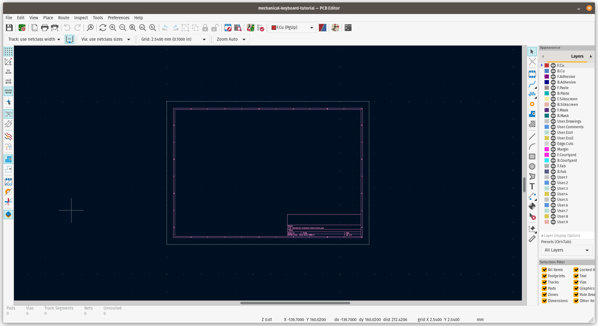
To open the PCB Editor, just press Ctrl + p or double-click the .kicad_pcb file, in this case mechanical-keyboard-tutorial.kicad_pcb.
Keyboard Shortcuts
- Spacebar - Reset Local Coordinates
- Ctrl+Z - Undo
- Ctrl+Y - Redo
- K - Track Display Mode
- Delete - Delete
- Backspace - Delete Track Segment
- X - Add New Track
- V - Add Via
- Ctrl+V - Add Microvia
- / - Switch Track Posture
- D - Drag Track, Keep Slope
- P - Place Item
- C - Copy Item
- End - End Track
- M - Move Item
- F - Flip Item
- R - Rotate Item
- G - Drag Item
- T - Get and Move Footprint
- L - Lock/Unlock Footprint
- Ctrl+S - Save Board
- Ctrl+L - Load Board
- Ctrl+F - Find Item
- End - Edit Item
- PgDn - Switch to Cooper Layer
- F5 - Switch to Inner Layer 1
- F6 - Switch to Inner Layer 2
- PgUp - Switch to Component Layer
- + - Switch to Next Layer
- - Switch to Previous Layer
- O - Add Module
- W - Switch Track Width to Next
- Ctrl+W - Switch Track Width to Previous
- H - Switch Highcontrast Mode
Grid Configuration
The most common grid size in mechanical keyboard is 19.05 x 19.05, and we will use that number and divide by 4 or 8 to make us easier when moving and snapping all the footprints in the drawing sheet.
Why not exactly 19.05? We need the smaller factor possible to place tiny components and routing, the larger the number will make it difficult to move the components or the routing.
Find the Grid options, and scroll down to choose Edit User Grid...
Fill with 19.05/4 or 19.05/8 in the User Defined Grid section, and it will automatically calculate the number when cursor move from the field. Then press OK
I use
19.05/8on this example
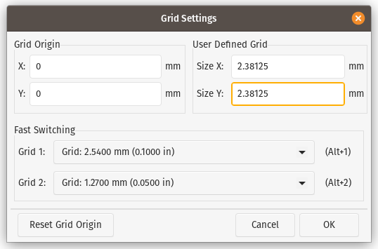
Next, back to the Grid option, and scroll down to select the previously defined User Grid
Updating PCB from Schematic
To add all the footprints, we need to update the PCB Editor from what changed in Schematic Editor, on the keyboard, press F8 or click this button on toolbar.
Click Update PCB button on the new prompt with default configuration.
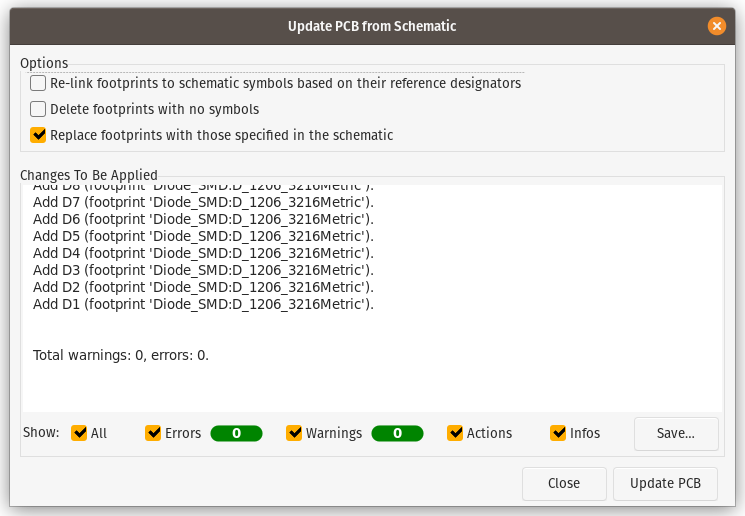
On the PCB Editor, just place all the imported footprints to the drawing sheet.
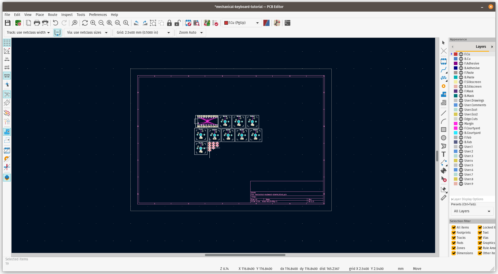
Arrange the footprint
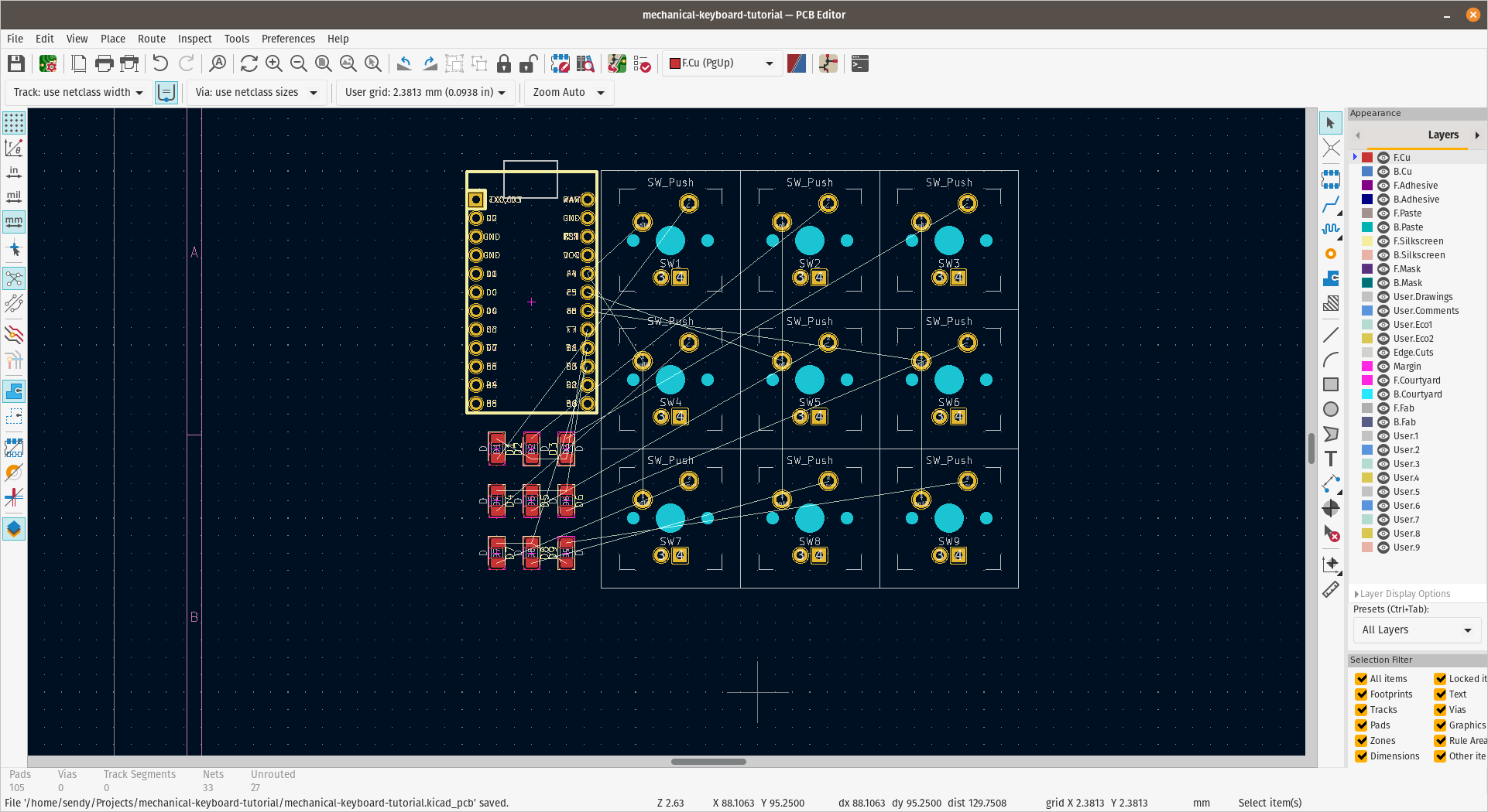
Back to the previous design preview, we will have 3x3 pad, and the ProMicro will sit on the left side. Just arrange the footprint on the drawing side.
|------|---|---|---|
|      | 7 | 8 | 9 |
|      |---|---|---|
| Pro  | 4 | 5 | 6 |
| Micro|---|---|---|
|      | 1 | 2 | 3 |
|------|---|---|---|
|------|---|---|---|
|      |SW1|SW2|SW3|
|      |---|---|---|
| MCU1 |SW4|SW5|SW6|
|      |---|---|---|
|      |SW7|SW8|SW9|
|------|---|---|---|
The final design / product is up to you, this is for demo purpose only
PCB Cut
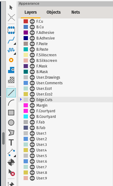
All footprints are in place, time to define the PCB edges so we can cut the PCB following the line. Select Edge.Cuts layer from the right sidebar in Layers tab, then Draw a Line or press Ctrl+Shift+L, next step is to pull the line and draw the PCB cut.
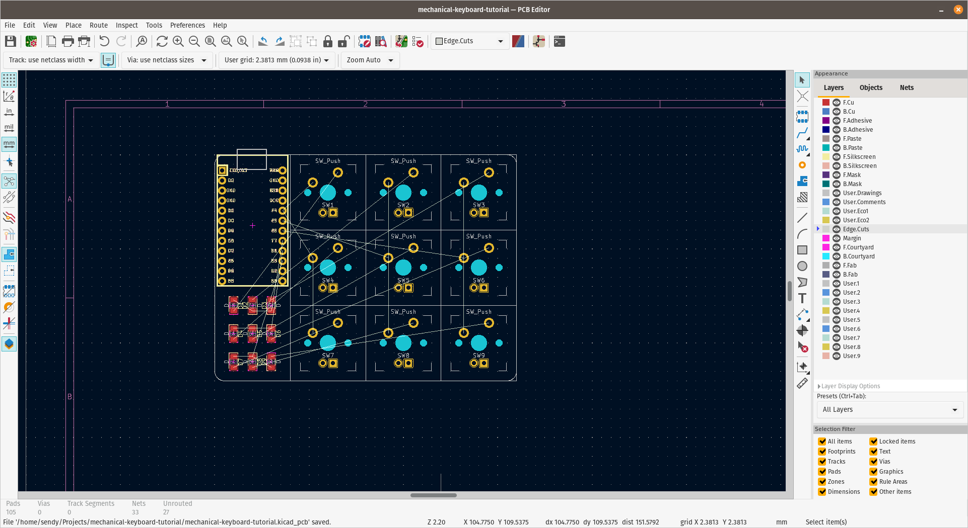
if you want rounded edge, play it and combine with Draw an arc tool, make sure all edges are snap each other.
Ground Plane
Next is to put ground plane to reduce electrical noise in PCB circuits. To add a ground plane, set F.Cu or B.Cu as active layer and press Add a filled zone or Ctrl+Shift+Z, and click where the ground plane start covering in drawing sheet, select F.Cu and B.Cu in Layer selection and GND in Net selection.
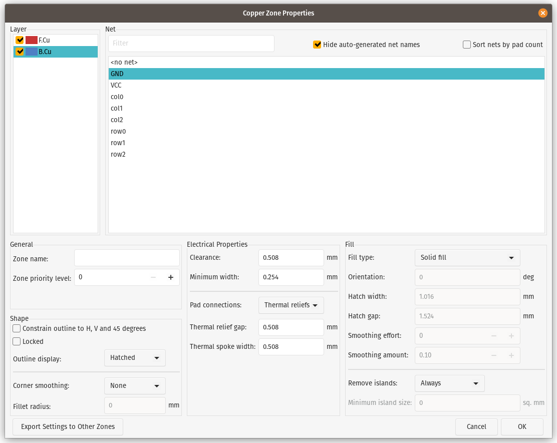
Draw the area covering whole PCB.
To cover whole PCB with GND fills, press B, to remove it press Ctrl+B.
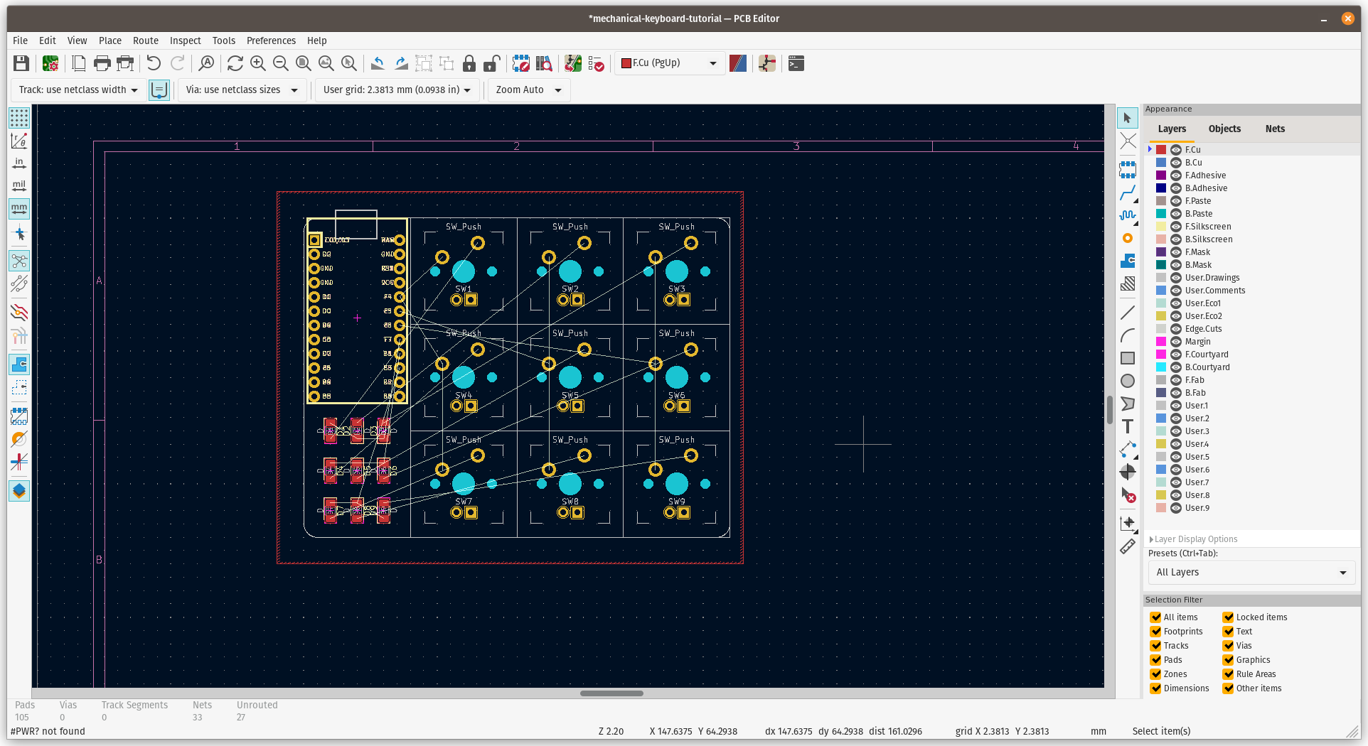
Routing
You see we have virtual line with white color, we call it Ratsnest, this indicate the pad aren't connected correctly to their counterparts, we need to connect those with a routing line.
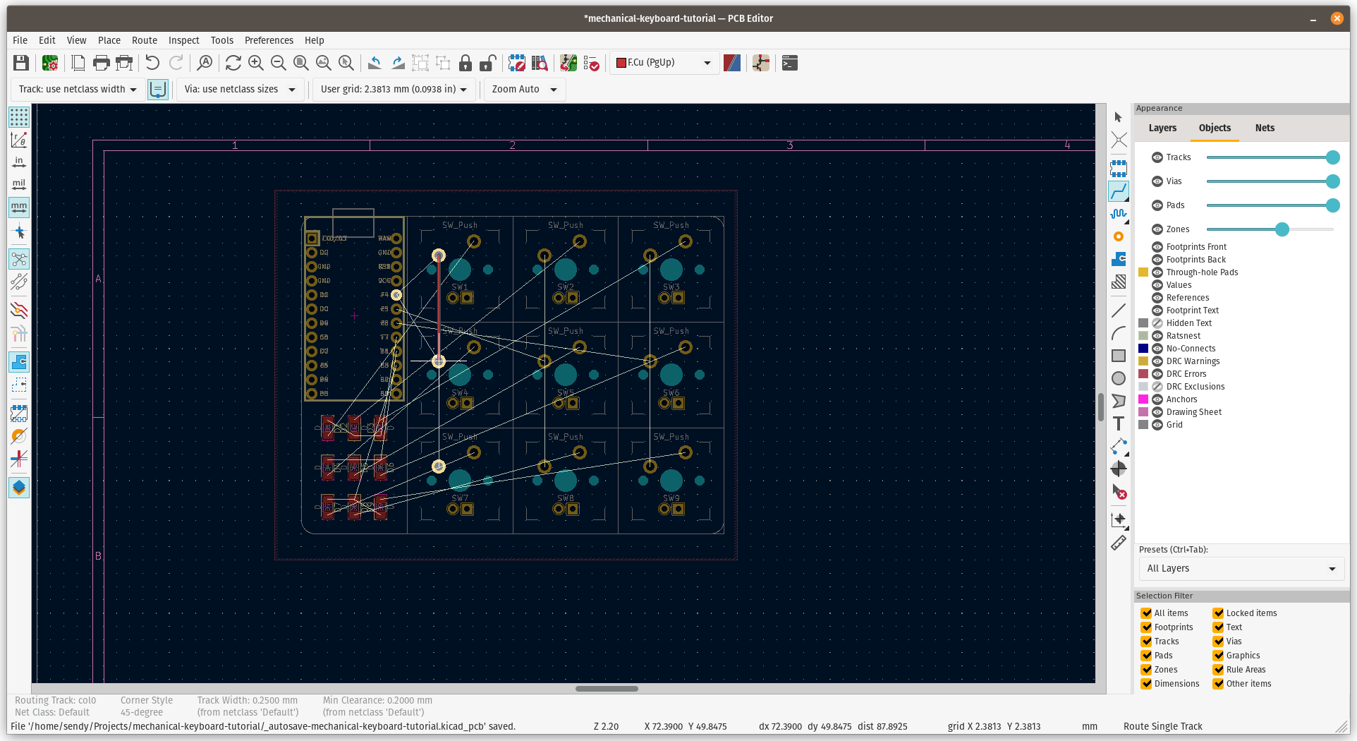
Activate Route tracks tool by press this icon or press X
Follow the Ratsnest to connect all the pads.
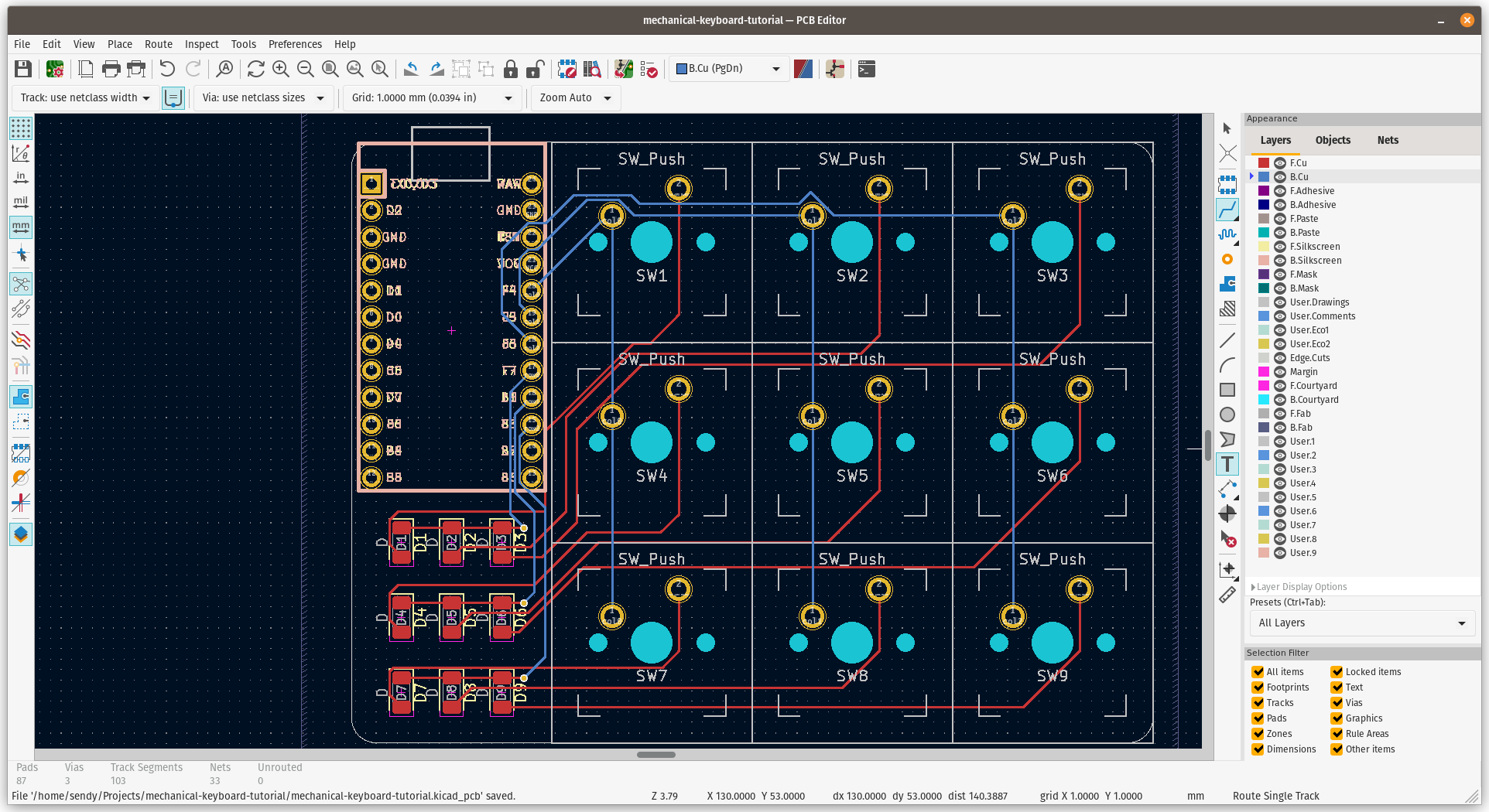
If you have difficulties to route because of layer conflicts, just use via hole
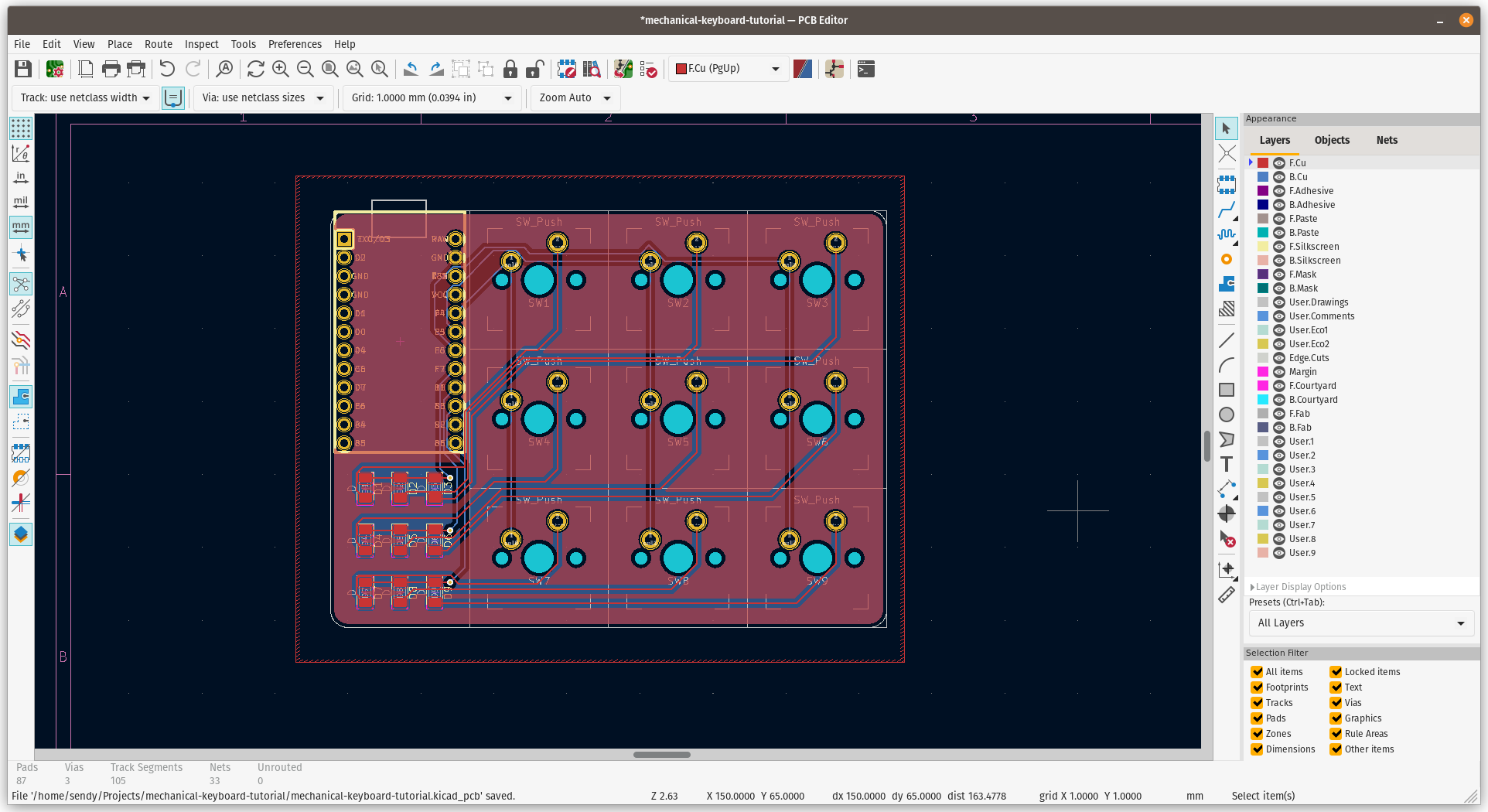
After all routes are connected, refill again the PCB by pressing B.
3D Viewer
KiCad have built in 3D preview, press Alt+3 to open the PCB preview. On this window, you can inspect and preview all components or footprints in PCB, it also have 3D models for supported footprint.
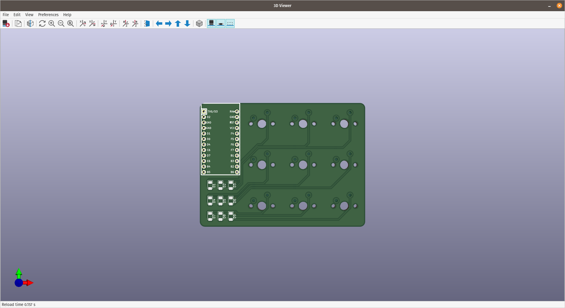
Congratulations! Now you have a macropad PCB!